Latches
Table of contents
- Latches
- Introduction
- Differences between latches and flip-flops
- Sub-modules
- Introduction
- State table
- Introduction
- State table
- Introduction
- State table
- Introduction
- State table
Latches
Introduction
There are two types of memory elements based on the type of triggering that is suitable to operate it.
- Latches
- Flip-flops
Latches operate with enable signal, which is level sensitive. Whereas, flip-flops are edge sensitive. Let’s discuss about flip-flops in next module. Latches are basic storage elements that operate with signal levels (rather than signal transitions). They are level-sensitive devices, that are useful for the design of the asynchronous sequential circuits. They, generally, have 2 inputs and 1 output pins. And the process where the output of the circuit depends on the previous state and the present input value(s) supplied, with the output value being constant (changing only for a particular condition in the input(s)), is referred to as latching.
Differences between latches and flip-flops
| Latches | Flip-flops |
|---|---|
| Level triggered | Edge triggered |
| Asynchronous device | Synchronous device |
| Doesn’t contain clock signal | Contains a clock signal |
| It will change its state as long as it is enabled | It will change its state only during a given clock cycle |
| Consumes less power | Consumes more power |
| Faster | Slower |
| Examples: D-Latch, T-Latch | Examples: D-Flip flop, T-Flop flop |
Sub-modules
Now, let us discuss about SR Latch, D Latch, JK Latch & T Latch one by one.
SR latch
Introduction
SR Latch is also called as Set Reset Latch. This latch affects the outputs as long as the enable, E is maintained at ‘1’. The circuit diagram of SR Latch is shown in the following figure.
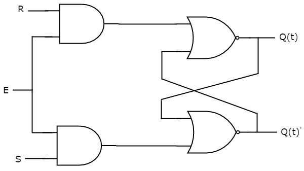
This circuit has two inputs S & R and two outputs Q(t) & Q(t)’. The upper NOR gate has two inputs R & complement of present state, Q(t)’ and produces next state, Q(t+1) when enable, E is ‘1’. Similarly, the lower NOR gate has two inputs S & present state, Q(t) and produces complement of next state, Q(t+1)’ when enable, E is ‘1’.
A 2-input NOR gate produces an output, which is the complement of another input when one of the input is ‘0’. Similarly, it produces ‘0’ output, when one of the input is ‘1’.
-
If S = 1, then next state Q(t + 1) will be equal to ‘1’ irrespective of present state, Q(t) values.
-
If R = 1, then next state Q(t + 1) will be equal to ‘0’ irrespective of present state, Q(t) values.
At any time, only of those two inputs should be ‘1’. If both inputs are ‘1’, then the next state Q(t + 1) value is undefined.
State table
| S | R | Q(t+1) |
|---|---|---|
| 0 | 0 | Q(t) |
| 0 | 1 | 0 |
| 1 | 0 | 1 |
| 1 | 1 | - |
Therefore, SR latch performs three types of functions such as Hold, Set & Reset based on the input conditions.
D latch
Introduction
There is one drawback of SR Latch. That is the next state value can’t be predicted when both the inputs S & R are one. So, you can overcome this difficulty by D Latch. It is also called as Data Latch. The circuit diagram of D Latch is shown in the following figure.
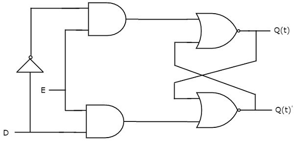
This circuit has single input D and two outputs Q(t) & Q(t)’. D Latch is obtained from SR Latch by placing an inverter between S amp;& R inputs and connect D input to S. That means the combinations, having same values, of S & R are eliminated.
-
If D = 0 → S = 0 & R = 1, then next state Q(t + 1) will be equal to ‘0’ irrespective of present state, Q(t) values. This is corresponding to the second row of SR Latch state table.
-
If D = 1 → S = 1 & R = 0, then next state Q(t + 1) will be equal to ‘1’ irrespective of present state, Q(t) values. This is corresponding to the third row of SR Latch state table.
State table
| D | Q(t + 1) |
|---|---|
| 0 | 0 |
| 1 | 1 |
Therefore, D Latch Hold the information that is available on data input, D. That means the output of D Latch is sensitive to the changes in the input, D as long as the enable is High.
In this module, you implemented various Latches by providing the cross coupling between NOR gates. Similarly, you can implement these Latches using NAND gates.
JK latch
Introduction
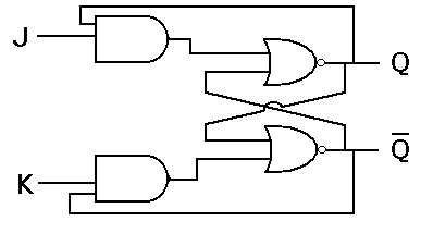
JK latch is similar to RS latch. This latch consists of 2 inputs J and K as shown in the below figure. The ambiguous state has been eliminated here: when the inputs of Jk latch are high, then output toggles. The output feedback to inputs is the only difference that can be seen here, which is not there in the RS latch.
State table
| J | K | Q(t+1) |
|---|---|---|
| 0 | 0 | Q(t) |
| 0 | 1 | 0 |
| 1 | 0 | 1 |
| 1 | 1 | Q(t)’ |
T latch
Introduction
T latch is formed when the inputs of the JK latch are shorted. When the input is high, then the output toggles.
State table
| T | Q(t) | Q(t+1) |
|---|---|---|
| 0 | 0 | 0 |
| 0 | 1 | 1 |
| 1 | 0 | 1 |
| 1 | 1 | 0 |
- The inputs of an SR latch includes ?
- 1 input & 3 outputs
- 4 inputs only
- 3 inputs & 1 output
- 2 inputs & 2 outputs
- From which latch does D latch is obtained ?
- JK latch
- T latch
- SR latch
- None of the above
- JK latch is similar to ?
- T latch
- D latch
- RS latch
- None of the above
- When the T latch output will toggle ?
- Input is low
- Input is high
- Output is high
- Output is low
- Input is low