Registers
Table of contents
- Introduction
- Serial-in serial-out
- Serial-in parallel-out
- Parallel-in serial-out
- Parallel-in parallel-out
- Applications of shift registers
Introduction
A Flip-flop is a 1 bit memory cell which can be used for storing the digital data. To increase the storage capacity in terms of number of bits, you can use a group of flip-flops. Such a group of flip-flops is known as a Register. The n-bit register will consist of n number of flip-flop(s) and it is capable of storing an n-bit word.
The binary-data, in a register, can be transfered within itself from one flip-flop to another. A shift register is a type of register that allows such data transfers. Shift register has 4 modes of operations.
Next, let us have a look at each register operation one by one.
Serial-in serial-out
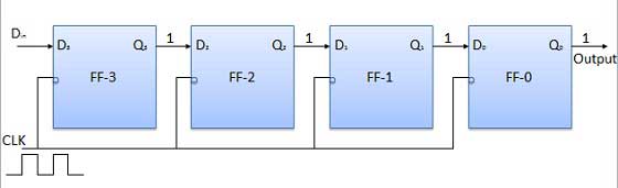
Let all the flip-flops be initially in the reset condition i.e. Q3 = Q2 = Q1 = Q0 = 0. If an entry of a four-bit binary number 1 1 1 1 is made into the register, this number should be applied to Din bit with the LSB bit applied first. The D input of FF-3 i.e. D3 is connected to serial data input Din. The output of FF-3 i.e. Q3 is connected to the input of the next flip-flop i.e. D2, and so on.
Block diagram
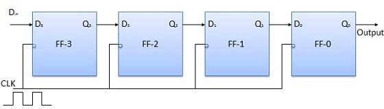
Operation
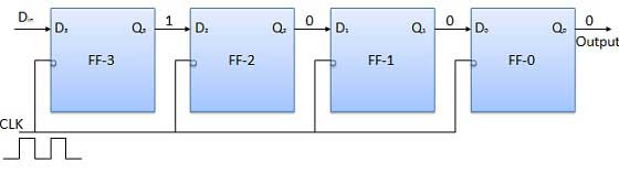
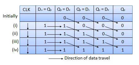
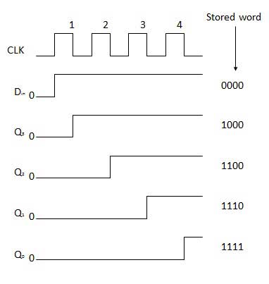
Before application of the clock signal, let Q3 Q2 Q1 Q0 = 0000 and apply the LSB bit of the number to Din. So Din = D3 = 1. Now, apply the clock. On the first falling edge of the clock, the FF-3 is set, and stored word in the register is Q3 Q2 Q1 Q0 = 1000.
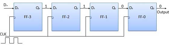
Apply the next bit to Din. So Din = 1. As soon as the next negative edge of the clock gets triggered, FF-2 will set and the stored word change to Q3 Q2 Q1 Q0 = 1100.
Apply the next bit to be stored i.e. 1 to Din. Apply the clock pulse. As soon as the third negative clock edge gets triggered, FF-1 will be set and output will get modified to Q3 Q2 Q1 Q0 = 1110.
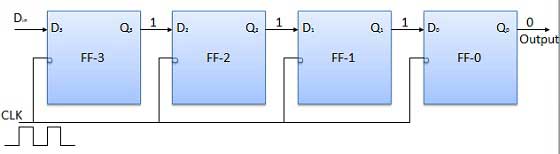
Similarly with Din = 1 and with the fourth negative clock edge arriving, the stored word in the register is Q3 Q2 Q1 Q0 = 1111.
Truth table
Waveforms
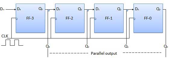
Serial-in parallel-out
-
In such types of operations, the data is entered serially and taken out in parallel fashion.
-
Data is loaded bit-by-bit. The output(s) are disabled as long as the data is loading.
-
As soon as the data loading gets completed, all the flip-flops contain their required data. The output(s) are enabled so that all the loaded data is made available over all the output lines at the same time.
-
4 clock cycles are required to load a four-bit word. Hence the speed of operation of SIPO mode is the same as that of the SISO mode.
Block diagram
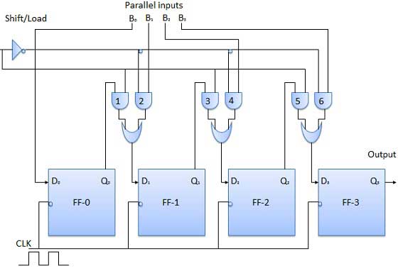
Parallel-in serial-out
-
Data bits enter in a parallel fashion.
-
The circuit, shown below, is a four-bit parallel-in serial-out register.
-
Output of the previous flip Flop is connected to the input of the next one via a combinational circuit.
-
The binary input data bits B0, B1, B2, B3 are applied through the same combinational logic circuit.
-
There are two modes in which this circuit can work, namely - shift mode and load mode.
Load mode
When the shift/load bar line is low (0), the AND gates 2, 4 and 6 become active, and they will pass B1, B2, B3 bits to the corresponding flip-flops. On the low going edge of the clock, the binary inputs B0, B1, B2, B3 will get loaded into the corresponding flip-flops. Thus, the parallel loading takes place.
Shift mode
When the shift/load bar line is low (1), the AND gates 2, 4 and 6 become inactive. Hence, the parallel loading of the data becomes impossible. But the AND gates 1,3 and 5 become active. Therefore the shifting of data takes place from left-to-right bit-by-bit on the application of clock pulses. Thus, the parallel-in serial-out operation takes place.
Block diagram
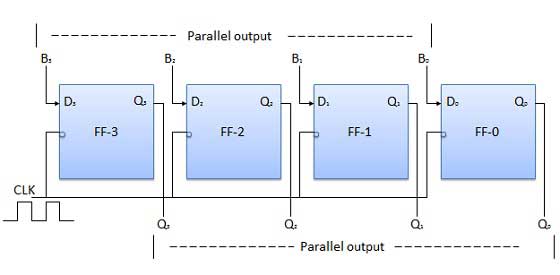
Parallel-in parallel-out
Here, the 4-bit binary datda inputs B0, B1, B2, B3 are applied to the data inputs D0, D1, D2, D3, respectively, of the four flip-flops. When a negative edge of the clock is triggered, then the flip-flops get loaded with the input binary bits simultaneously. The loaded bits appear at the output side, simultaneously, as well. Only the clock pulse is essential to load all the binary bits.
Block diagram
Applications of shift registers
Overview
Shift registers are sequential circuits used primarily used for:
- Storage of Data
- Data transfer through movement of binary data
- Data manipulation
- Counter implementation
They are called shift registers as it moves or shifts binary input data to its output per clock cycle. Shift registers are commonly used to store data inside calculators. Even in computer systems, operations like addition, subtraction, division and multiplication are performed by registers.
Shift registers can be applied in the following ways:
-
Parallel to Serial conversion: Used in transmitters after analog to digital conversion in order to convert parallel input data into serial data
-
Serial to Parallel conversion: Used in receivers before digital to anlogous conversion takes place in order to convert serial input data into parallel data
-
Sequence Generator: Generate a sequence of 0s and 1s when combined with some additional gates
-
Counters: Shift registers can be implemented as counters based on the output of the rightmost D flip-flop that is connected to the serial input, namely the Ring Counter and the Johnson Ring Counter
-
Serial-in Serial-out registers are used for time delays
Ring counter
Similar to how the Serial-in Serial-out register requires ‘N’ clock pulses to shift N bit data, the ‘N’ Ring Counter produces a sequence of 0s and 1s, by having the rightmost D flip-flop as input to the leftmost D flip-flop as opposed to applying data externally. That is, the output of the last flip-flop is connected to the output of the first flip-flop in the ring. These patterns of states (0s and 1s) are repeated every ‘N’ clock cycles.
The number of states in a Ring Counter are directly proportional to the number of flip-flops used.
The block diagram of the 3-bit Ring counter is shown in the following figure.
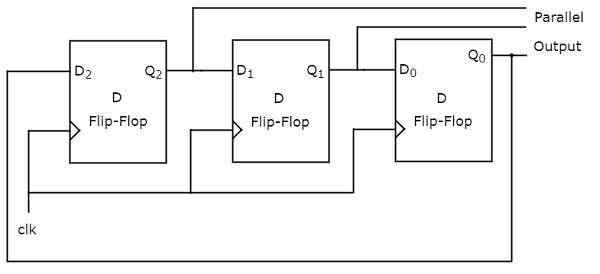
A 3-bit Ring Counter will contain only a 3-bit SIPO shift register.
Assume, the initial status of the D flip-flops from leftmost to rightmost is Q2Q1Q0=001. Here, Q2 & Q0 are MSB & LSB respectively. You can understand the working of Ring counter from the following table.
| No of positive edge of Clock | Serial Input = Q0 | Q2(MSB) | Q1 | Q0(LSB) |
|---|---|---|---|---|
| 0 | - | 0 | 0 | 1 |
| 1 | 1 | 1 | 0 | 0 |
| 2 | 0 | 0 | 1 | 0 |
| 3 | 0 | 0 | 0 | 1 |
Due to the absence of the clock signal, the initial status of the D flip-flops is Q2Q1Q0=001. This state will repeat every third positive edge transition of the clock signal.
Similarly, the following operations take place every positive edge of the clock cycle:
-
Serial input of the first D flip-flop gets the previous output of the third flip-flop. Thus, the present output of the first D flip-flop is equal to the previous output of the third flip-flop.
-
The previous outputs of first and second D flip-flops are right-shifted by one bit. That implies that the present outputs of second and third D flip-flops are equal to the previous outputs of first and second D flip-flops.
Johnson ring counter
The Johnson ring counter functions similarly to the Ring counter. The difference being that the complemented output of rightmost D flip-flop is given as input of leftmost D flip-flop instead of normal output. Thus, ‘N’ bit Johnson Ring counter produces a sequence of states (pattern of zeros and ones) and it repeats for every ‘2N’ clock cycles.
Johnson ring counter is also called the Twisted ring counter and Switch tail ring counter. The block diagram of 3-bit Johnson Ring counter is shown in the following figure.
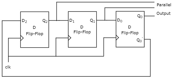
The 3-bit Johnson Ring counter also contains only a 3-bit SIPO shift register.
Assume, initially, all the D flip-flops are cleared. So, Q2Q1Q0=000. Here, Q2 is the MSB & Q0 is the LSB.
| No of positive edge of Clock | Serial Input = Q0 | Q2(MSB) | Q1 | cQ0(LSB) |
|---|---|---|---|---|
| 0 | - | 0 | 0 | 0 |
| 1 | 1 | 1 | 0 | 0 |
| 2 | 1 | 1 | 1 | 0 |
| 3 | 1 | 1 | 1 | 1 |
| 4 | 0 | 0 | 1 | 1 |
| 5 | 0 | 0 | 0 | 1 |
| 6 | 0 | 0 | 0 | 0 |
The initial status of the D flip-flops in the absence of the clock signal is Q2Q1Q0=000. This status repeats for every six positive edge transitions of the clock signal.
Similarly, the following operations take place for every positive edge of the clock signal.
- Serial input of first D flip-flop gets the previous complemented output of the third flip-flop. So, the present output of the first D flip-flop is equal to the previous complemented output of the third flip-flop.
- The previous outputs of first and second D flip-flops are right shifted by one bit. That means, the present outputs of second and third D flip-flops are equal to the previous outputs of first and second D flip-flops.